Transistor
Brief description
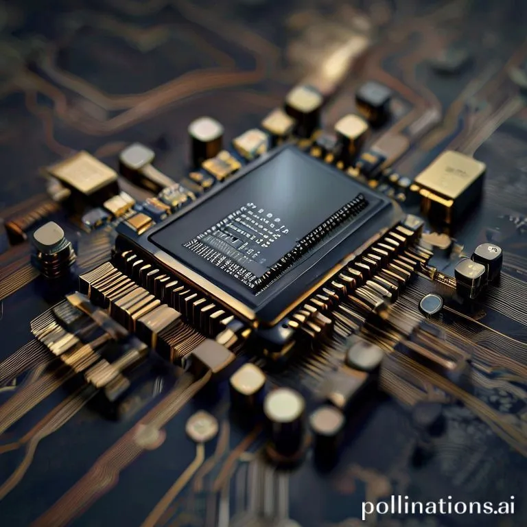
The transistor is a semiconductor device used to amplify or switch electrical signals and power. It is the fundamental building block of Basic Electronics, replacing bulky and fragile Vacuum Tubes. It allows for the miniaturization of electronic circuits and is the basis for everything from simple Radios to complex computers.
Use / Function
Its practical purpose is to control the flow of electricity:
- Amplification: Takes a weak input signal and boosts it to a stronger output signal (essential for radios, audio, and communications).
- Switching: Acts as an electronic switch, turning current on or off completely based on a control signal. This is the foundation of binary logic (0s and 1s) in computing.
- Oscillation: Can generate continuous signals of a specific frequency when combined with other components (clocks, radio transmitters).
- Voltage Regulation: Maintains steady voltage levels in power supplies.
Operating principle
The transistor relies on the quantum properties of semiconductor materials, primarily Silicon (Si) or Germanium (Ge).
- Semiconductors: These materials are neither perfect conductors nor insulators. Their conductivity can be modified by adding impurities (“doping”).
- Doping:
- N-type: Doped with materials that have extra electrons (negative charge carriers), like Phosphorus.
- P-type: Doped with materials that have “holes” (positive charge carriers), like Boron.
- The Junction: When N-type and P-type materials are joined, they form a junction. By applying voltage to specific terminals, you can control the flow of electrons across these junctions.
Main Types:
- BJT (Bipolar Junction Transistor): Has three terminals: Base, Collector, and Emitter. A small current at the Base controls a large current flowing from Collector to Emitter. It’s like a small valve controlling a large pipe.
- FET (Field Effect Transistor): Has three terminals: Gate, Source, and Drain. Voltage at the Gate creates an electric field that pinches or opens the channel between Source and Drain. It draws almost no current to control the flow, making it very efficient.
How to create it
Warning: Manufacturing reliable transistors requires industrial-level precision, clean rooms, and dangerous chemicals. It is likely impossible to manufacture modern integrated circuits in a post-collapse scenario without restoring industrial infrastructure. However, primitive point-contact transistors (like the first ones invented in 1947) are theoretically possible but extremely difficult.
Primitive Point-Contact Transistor (Theoretical Survival Approach):
- Material Preparation: You need a crystal of high-purity Germanium (easier to work with than Silicon due to lower melting point and processing requirements).
- Base: A small slab of the germanium crystal serves as the base.
- Contacts: Two very fine metal wires (gold or phosphor bronze) must be pressed against the crystal surface very close to each other (micrometers apart).
- Forming: A high current pulse is sent through the wires to fuse them slightly to the crystal and create the necessary P-N junctions at the contact points.
Industrial Process (For context):
- Purification: Silicon is purified to 99.9999999%.
- Crystal Growth: Grown into a single large crystal (boule) and sliced into wafers.
- Photolithography: Patterns are projected onto the wafer using light and photoresist chemicals.
- Etching & Doping: Material is removed, and dopants are blasted into the exposed areas to create N and P regions.
- Metallization: Microscopic wires are laid down to connect the components.
Materials needed
- Semiconductors:
- Germanium: Easier for primitive attempts (lower melting point, historically first).
- Silicon: Standard for modern tech, but requires extreme heat and purity.
- Dopants:
- Arsenic, Phosphorus, Antimony (N-type).
- Boron, Gallium, Indium (P-type).
- Contacts/Conductors:
- Gold (resists corrosion, malleable for fine wires).
- Copper, Aluminum.
- Substrate: Insulating material for mounting.
Variants and improvements
- Vacuum Tubes: The predecessor. Much easier to build manually (glassblowing, metal wire) but bulky, hot, and fragile.
- Point-Contact Transistor: The first transistor type. Unstable and noisy, but the most “low-tech” version.
- Junction Transistor: Improved stability by sandwiching layers (NPN or PNP) rather than pressing wires.
- MOSFET: The modern standard. High efficiency, fast switching, basis of all modern processors.
Limits and risks
- Heat: Transistors are very sensitive to heat. They can undergo “thermal runaway” where heat causes more current, which causes more heat, until destruction.
- Static Electricity (ESD): A simple spark from your finger can permanently destroy a transistor by punching through its microscopic internal insulation.
- Voltage Spikes: Very sensitive to over-voltage.
- Radiation: High radiation can degrade or flip bits in transistors (relevant in nuclear scenarios).
- Scavenging Priority: Since manufacturing is near-impossible, transistors should be a high-priority scavenge item. They are durable if stored correctly (anti-static bags).